CDA-4101 Lecture 09 Notes
Sequential Circuits
- Combinational vs. Sequential
- sequential circuits have memory, so past inputs can be
remembered.
- gates are the fundamental building block of (many) memory
units.
Sequential Circuit State
- Since sequential circuit output can be influenced by any of its
past inputs, we need a way to remember the history of past inputs.
- Often, remembering the entire histoty is not feasible, or even
needed.
- The state of the system is a summary or subset of all the past
history of input that we will need in order to define the circuits
future output history.
- e.g., Remote control "up" and "down"channel buttons.
- Note that the state does not rule out the possibility of actually
storing the entire input history.
State Variables
- Sequential circuit state consists of a set of state
variables
- state variables are binary valued (0's and 1's)
- number of possible states is 2n where 'n' is the
number of state variables.
state transitions typically occur at time specified by a
free-running clock.
Clocks
- active high means that the state changes occur at the
rising edge of the clock.
- active low means that the state changes occur at the
falling edge of the clock.
|

|
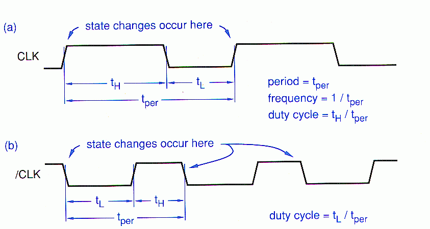
a) Active high b) Active low
Quartz Crystals
- quartz crystal oscillator is typically used to generate the
clock signal
- quartz is a piezoelectric crystal:
- bending the crystal causes voltages to run along its
surface
- applying voltage causes the crystal to bend
- with right shape and voltage you get the crystal oscillating at
a very precise frequency.
- just tap into the surface voltage to get an electronic signal
out of it.
- clock frequencies typically from 32 kHz to hundreds of MHz
- You can subdivide the clock cycles by inserting small
delays. (i.e., you don't need a quartz crystal operating at 2 GHz to
run a machine at that speed.)
|
|
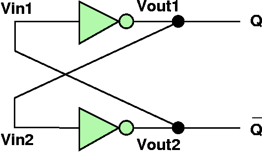
A Bistable Element
- simplest sequential circuit
- two stable states
- but no way to control it (no inputs)
- non-deterministic metastable state
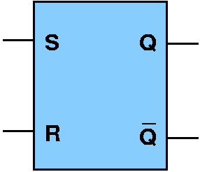
Latches
- Latch is the simplest form of memory (a.k.a. state
variable)
- SR Latch: S for "Set" and R for "Reset"
- If S = R = 1 then it enters an "unstable" state
| S | R | Q | Q' |
|---|
| 0 | 0 | last Q | last Q' |
| 0 | 1 | 0 | 1 |
| 1 | 0 | 1 | 0 |
| 1 | 1 | 0 | 0 |
|
|
Clocked SR Latch
- SR Latch is sensitive to change at any time.
- prefer to control "loading" of the latch at specific fixed
intervals.
- add an "enable" line to the circuit, usually connected to a
clock
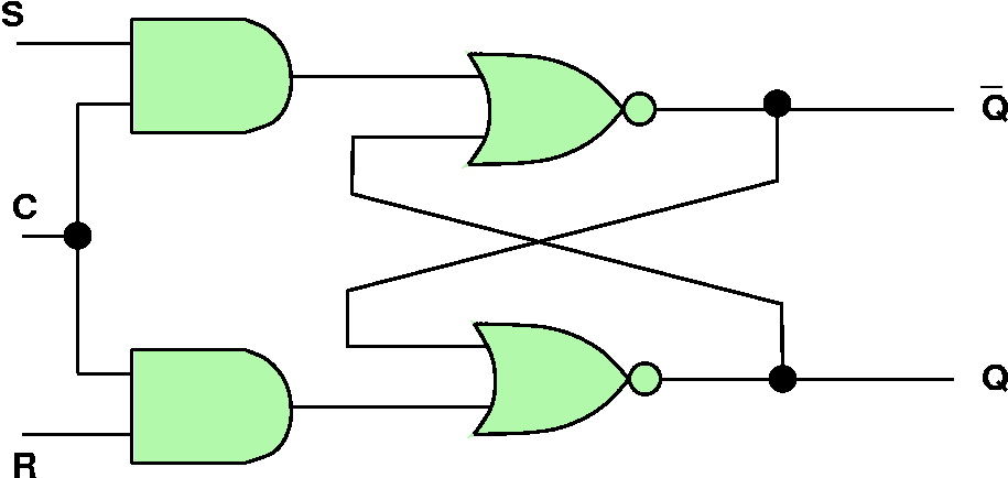
|
| S | R | C | Q | Q' |
|---|
| 0 | 0 | 1 | last Q | last Q' |
| 0 | 1 | 1 | 0 | 1 |
| 1 | 0 | 1 | 1 | 0 |
| 1 | 1 | 1 | 0 | 0 |
| x | x | 0 | last Q | last Q' |
|
|
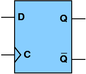
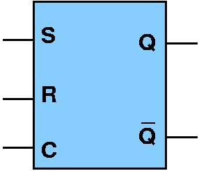
D Latch
- some digital design situations lend themselves to separate
control of "set" and "reset"
- but if we simply want to store a bit of information, we only
want/need one control input.
- Want also prefer to remove the situation where S = R = 1 leads
to unpredictable state
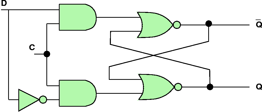
|
| D | C | Q | Q' |
|---|
| 0 | 1 | 0 | 1 |
| 1 | 1 | 1 | 0 |
| x | 0 | last Q | last Q' |
|
|
Truth Table Shorthand Notation
For the truth tables for the latches/flip-flops, you see things in the
notes that show:


  D  C  |     Q        Q'
 ==========================
  0  1  |     0        1
  1  1  |     1        0
  x  0  |  last Q   last Q'

First off, this is a shorthand for:

  D  C  |     Q        Q'
 ==========================
  0  1  |     0        1
  1  1  |     1        0
  0  0  |  last Q   last Q'
  1  0  |  last Q   last Q'

Then, more importantly, this table itself is itself a shorthand for
the full truth table.  The full truth table will have all the possible
inputs on the left and the outputs on the right.  For a sequential
circuit, the world of possible inputs includes not just the regular
inputs, but the current state of the circuit as well.  Thus, the full
truth table in this case is:

  D   C   current Q   current Q'   |   next Q   next Q'
==========================================================
  0   0      0           0         |     0        0
  0   0      0           1         |     0        1
  0   0      1           0         |     1        0
  0   0      1           1         |     N/A      N/A
  0   1      0           0         |     0        1
  0   1      0           1         |     0        1
  0   1      1           0         |     0        1
  0   1      1           1         |     N/A      N/A
  1   0      0           0         |     0        0
  1   0      0           1         |     0        1
  1   0      1           0         |     1        0
  1   0      1           1         |     N/A      N/A
  1   1      0           0         |     1        0
  1   1      0           1         |     1        0
  1   1      1           0         |     1        0
  1   1      1           1         |     N/A      N/A
Edge-triggered Flip Flops
- With latches, care must be taken that inputs are held stable
during entire time clock signal is high.
- more often, you'd like to load the latch at a single point in
time.
- a flip flop is a latch that is edge triggered: only
loads values at a very small interval of time.
- can be either the rising or falling edge of the clock
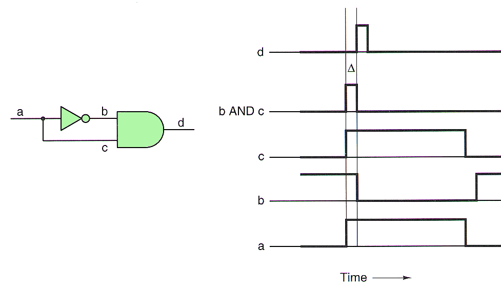
Circuit to get an "edge triggering"
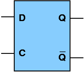
D Flip Flop
Real-world Latches and Flip flops
- there are many subtle timing issues that we have ignored
- there are more efficient and sophistated ways to build these
circuits which is usually what is done in reality
- fundamental ideas are all the same as these simpler circuits
- usually flip-flops have a separate "clear" signal as input
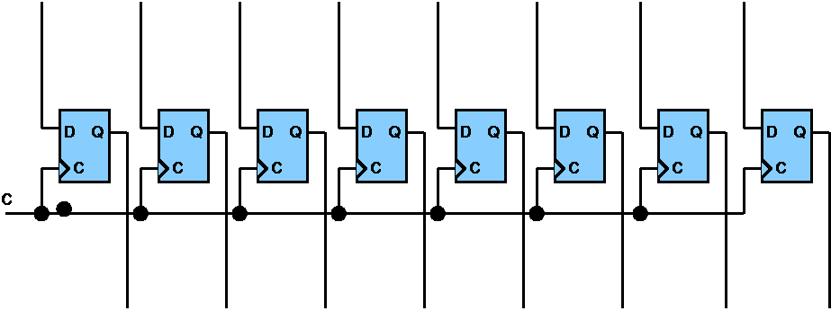
8 Bit Register
- A collection of two or more D flip flops tied to a common clock
is a register
- usually have a "clear" and "output enable" control inputs as
well.

Memories
- as more and more memory cells are desired, we need a way to
organized the memory elements that will keep the number of pin
(inputs/outputs) to a minimum.
- Memory sizes 2n x m: 'n' addressable locations and
'm' data lines
4x3 Memory
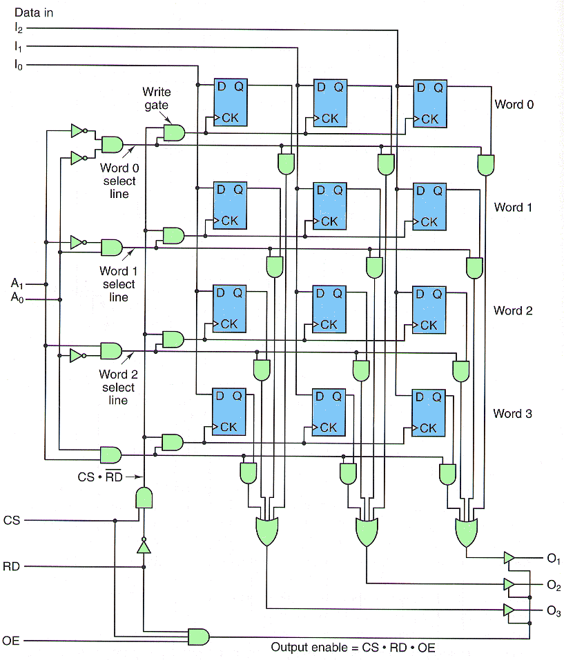
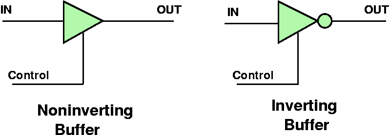
Inverting and Non-inverting Buffers
- to reduce the required pins further, the same ones are used to
output on a read and input on a write.
- this requires some special gate to make sure we are not putting
output on the same line as we are trying to input
- when control is low, acts like a broken circuit (high Z state)
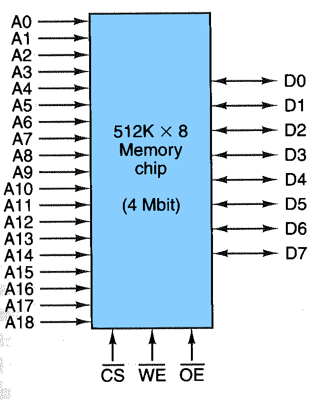
Memory Chips Example: 512K x 8
- 8 bit cells
- 512K Addressable locations
- 19 address lines
- CS = chip select
- WE = write enable
- OE = output enable
|
|
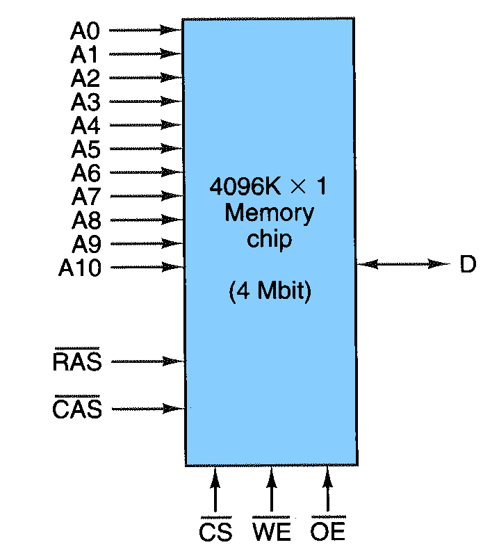
Memory Chips Example: 4096K x 1
- 1 bit cells
- arranged as an 211 x 211 matrix internally
- 11 address lines
- sequenced addressing: first row, then column
- RAS = Row Address Strobe
- CAS = Column Address Strobe
- slower access due to addressing
- less pins
- this row-then-column addressing means there needs to be a
register inside to remember the last row (i.e., it has its own
internal state)
|
|
Static RAM (SRAM)
- Static RAM is based on flip-flops
- Used for registers and caches
- very fast
- data stays intact as long as power is supplied
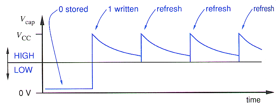
Dynamic RAM (DRAM)
- most regular RAM is DRAM
- Dynamic RAM uses a different technology (not flip-flops)
- uses a single transitor and a very small capacitor
- can pack many more of these into a chip than SRAM (SRAM needs 4
to 6 transitors)
- capacitor is charged, but then discharges at a particular rate
- to maintain memory, it must be periodically refreshed (every few
milliseconds)
- can refresh entire rows in one operation instead of having to
cycle through every possible memmory location
|
|
DRAM Perspective
- first DRAMs in the early 1970's
- all PCs use DRAM for their main system memory
- caching technologies have made more memory a smarter choice than
faster memory.
- only 5-10% of the data requirements of the processor are typically
supplied from the memory itself
DRAM Types
- previous discussion is "plain vanilla" conventional DRAM and is
mostly obsolete
Fast Page Mode (FPM) DRAM
- "page mode" preceded this but was quickly optimized to "fast
page mode" (differences have to do with specific timing of rowna nd
column addressing set-up times)
- slightly faster
- this is the technology where a single row address can be followed by
multiple column addresses
Extended Data Out (EDO) DRAM (a.k.a. HyperPage Mode)
- Allows minor amount of pipelining of memory accesses so one access
to the memory can begin before the last one has finished
- in real world performance it offers a minimal speed
increase over FPM memory
Burst Extended Data Out (BEDO) DRAM
- One access would generate 3 consecutive address
- eliminated continual column addressing for consecutive locations
- this technology bever went anywhere because SDRAM was just
emerging as the preferred technology ...
Asynchronous DRAM
- conventional DRAM, FPM, EDO and BEDO DRAM are all
asynchronous: they are not tied to a clock, but will simply
read/write data when control lines enable it
- asynchronous DRAM could not operate on a bus faster than about
66MHz
- processor must wait between memory accesses (typically about 60
ns)
Synchronous DRAM (SDRAM)
- synchronous DRAM is tied to system clock and allows one
request to generate a burst of memory reads (coordinated with the
clock cycle time)
- after request, results will be available in a fixed number of
clock cycles, so processor can do something else during cycles in
between.
- burst speed is for sequential memory accesses only
- also uses internal pipelining to improve performance
SDRAM Speed
- a 15 ns SDRAM actually has 60 ns or more total latency for a
given address
- comparing 15 ns SDRAM to 60 ns DRAM is comparing apples and
oranges
- the 15 ns is the pipeline cycle time, so you can get one
reference out of memory every 15 ns once the pipeline is full
- getting a single memory locations is actually slower than DRAM
(i.e., longer latency)
- SDRAM chips are officially rated in MHz so that there is a
common denominator between the bus speed and the chip speed.
SDRAM Types
Standard Synchronous DRAM (a.k.a., PC-66, JEDEC)
- The original SDRAM modules either used 83MHz chips (12ns) or 100MHz
chips (10ns)
- these were only rated for 66MHz bus operation due to barious
synchronization issues
PC-100
- Intel decided to clear up all the SDRAM timing issues with a
specification to support their true 100 MHz bus
- more than just the clock speed matters, so buyers had to be
careful about quality of PC-100 RAM
PC-133
- like PC-100, but slightly faster
Enhanced SDRAM (ESDRAM)
- small amount of SRAM cache which allows for lower latency times
and burst operations up to 200MHz
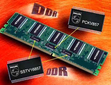
DDR (Double Data Rate)
- allows the activation of output operations on the chip to occur
on both the rising and falling edge of the clock
- can effectively double the speed of operation
- PC-100 DDR -> 200 MHz (PC-200)
- PC-133 DDR -> 266 MHz (PC-266)
|
|
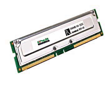
Direct Rambus DRAM (RDRAM or DRDRAM)
- a somewhat newer specification for memory design
- theoretically up to 800 MHz, but currently only up to 200 MHz
- the voltage level is much lower: 0-3.3 Volts on SDRAM and 0-2.2
Volts on Rambus. It takes less time to charge( or discharge) the
DRAM cell data storage capacitor to 2.2V than 3.3V
- 4 banks of interleved memory to help pipelining
- increased bandwidth, but not improved latency, which is the
current limiting factor (memory bandwidth is typically underutilized
in today's machines)
- more overhead than SDRAM to set up an accesses
- proprietary specification, requiring royalties, so a major
obstacle to adoption
|
|
Video DRAM (VRAM)
- video graphics have spawned the creation of several new,
innovative memory technologies specifially for video RAM (VRAM)
- based on asynchronous DRAMs
- many of them designed to allow the memory to be accessed by the
processor and read by the video card's refresh circuitry
simultaneously.
- This is called dual porting
- faster and more expensive than other DRAMs.
|
|
ROM (Read Only Memory)
- read-only
- non-volatile
- security
- e.g., older system BIOS (non-flashable BIOS)
|

|
PROM (Programmable ROM)
- write-once (programmable)
- special equipment to create
- usually use fuses that are burnt out like in a PLA
- analogous to CD-R
|

|
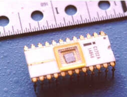
EPROM (Erasable PROM)
- erasable
- ultraviolet light to erase
- analogous to CD-R/W
|
|
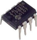
EEPROM (Electrically Erasable PROM)
- electronically erasable
- can be erased and programmed in place
- much slower than DRAMs/SRAMs (factor of 10)
- can be done in software
- e.g., system BIOS (flash BIOS)
|
|
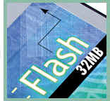
FLASH Memory
- newer type of EEPROM
- limited liftetime (10,000 or so erasures)
- used in cameras and many emerging applications
|
|